-
New hybrid strategy could unlock the use of organic compounds to convert body heat into electricity for portable devicesAlthough conjugated polymers are promising materials for many electronic applications, increasing their conductivity enough for efficiently converting heat to electricity has been tricky. Now, scientists from Ajou University, Korea, have devised a hybrid strategy that combines two existing doping methods to obtain unprecedented results. This could unlock the use of these polymers to power portable electronic devices and sensors using body heat.Thermoelectric conversion is a highly popular unconventional energy harvesting technique; theoretically, it allows for powering portable electronic devices and sensors using nothing but body heat. Many researchers have high hopes on conjugated polymers (CPs), special arrangements of long organic molecules that are used in flexible electronics, transistors, and solar cells. However, there are no effective methods to make CPs conductive enough for high efficiency thermoelectric energy conversion. Scientists at Ajou University, Korea, have recently pioneered a novel strategy that demonstrates extremely promising results. In their study, featured on the front cover of the latest issue of Advanced Functional Materials (Volume30, Issue42 2004598), they combined two of the best known methods for enhancing the conductivity of CPs into “hybrid doping”. This image, selected as the cover for Advanced Functional Materials, shows long strands of conjugated polymers doped to the max with F4TCNQ, a standard organic dopant Photo courtesy: Wiley Online Library In materials science, doping is the process of intentionally adding impurities to a material to enhance certain properties. For CPs, existing doping methods are “mixture blending” and “sequential doping.” In mixture blending, the polymer and the dopant are mixed in a solution, which is then spin coated to produce the doped CP. However, the amount of dopant that can be safely used without compromising the polymer structure is very small. Sequential doping, meanwhile, involves spin coating the CP first and then dipping it into a dopant solution. With this approach, the dopant can only penetrate the layers of the polymer at amorphous regions, leaving the crystalline areas undoped.The combined strategy is a straightforward fusion of both techniques; a pre-doped CP produced through mixture blending is dipped into a dopant solution. “Hybridizing both processes effectively maximizes the degree of doping of the CPs, yielding maximum conductivity without sacrificing other properties,” Professor Jong. H. Kim, who led the study, explains. The scientists compared CPs produced using each method in terms of their microscopic structure, optoelectrical properties, stability, and thermal conversion performance; the CPs processed with hybrid doping came out on top in all relevant areas. Excited about the results, Professor Kim comments: “Hybrid doping let us optimize the thermal energy conversion efficiency of existing and new CPs. In turn, this will eventually allow us to harvest waste heat from various sources, including the human body, to power all types of portable electronic devices and Internet-of-Things sensors.” This study is a huge step in the development of eco-friendly functional materials, and highly doped CPs will surely find their way into the electronic devices of tomorrow.ReferenceAuthors:Sang Eun Yoon1, Yeongkwon Kang2, Gyeong G. Jeon1, Dohyeon Jeon3, Sang Yeon Lee4, Seo-Jin Ko5, Taekyeong Kim3, Hyungtak Seo4, Bong-Gi Kim2, and Jong H. Kim1*Title of original paper:Exploring Wholly Doped Conjugated Polymer Films Based on Hybrid Doping: Strategic Approach for Optimizing Electrical Conductivity and Related Thermoelectric PropertiesJournal:Advanced Functional MaterialsDOI:10.1002/adfm.202004598Affiliations:1Department of Molecular Science and Technology, Ajou University2Department of Organic and Nano System Engineering, Konkuk University 3Department of Physics, Hankuk University of Foreign Studies4Department of Materials Science and Engineering and Department of Energy Systems Research, Ajou University5Division of Advanced Materials, Korea Research Institute of Chemical Technology*Corresponding author’s email: jonghkim@ajou.ac.kr About Ajou UniversityFounded in 1973, Ajou University has quickly grown to become one of the top universities in the Republic of Korea. With over 15,000 students and 50 research centers in diverse fields, Ajou University partakes in the largest national research and graduate education project funded by the Korean Ministry of Education. In line with its recently reformed vision, Ajou University’s goal is to change society by connecting minds and carrying out high-impact research to improve the welfare of people in and outside Korea. Website: https://www.ajou.ac.kr/en/index.do About the authorJong H. Kim (Jong Hyun Kim) is an Associate Professor of the Department of Molecular Science and Technology and the Department of Applied Chemistry and Biological Engineering at Ajou University. His group is developing new approaches to fabricate high-efficiency energy harvesting devices, including thermoelectric and photovoltaic devices. Professor Kim’s research group is also developing high-efficiency doping processes for transparent and stretchable electrodes for solar cells and NIR photodetectors. Before joining Ajou University, Jong H. Kim completed his postdoctoral training at Alex K.-Y. Jen’s lab at the University of Washington, USA. In 2011, he received a PhD in the Department of Materials Science and Engineering from Seoul National University, Korea.
-
20
- 작성자국제협력팀
- 작성일2021-02-03
- 4923
- 동영상동영상
-
A team of researchers including Ajou University’s Prof. Seo Hyung-tak has successfully developed an integrated optoelectronic diode capable of adapting, in a fashion similar to human visual perception, to various environments. The team’s discovery is expected to help develop visual devices with artificial nerves, intelligent photosensors, data processors, and innovations in robotics.Prof. Seo (Dept. of Materials Science and Engineering / Graduate Dept. of Energy Systems, pictured) has announced that his team has developed a photosensor diode capable of differentiating information processing depending on angles of perception. The team’s invention is discussed in detail in “Environment-Adaptable Photonic-Electronic Coupled Angular Perception System,” published in the October issue of ACS Nano (IF = 14.588). The team included two other members from Ajou: Prof. Kim Sang-wan (Dept. of Electrical and Computer Engineering) and Dr. Mohit Kumar (lead author).The human vision system is capable of adapting on its own to changes in its surroundings, including differences in lighting, by detecting changes in optic signals in real time. It is also capable of differentiating between visual signals from different angles of vision (up or down, left or right) and processing the obtained data accordingly. Human vision captures optical data and converts it into photoelectronic signals, which are then encoded into electric spikes of appropriate sizes. Information thus processed is then transmitted to the visual cortex and stored on the synaptic network.Numerous attempts have been made so far to develop artificial sight by simulating the complex and intricate workings of human visual perception. Success has been elusive so far, however, in developing artificial vision with a sufficiently simple structure and a rational energy demand.Much of the research on artificial sight circuits to date has focused on understanding and visualizing information under general lighting. Effective artificial sight, however, crucially requires a technology capable of recognizing objects from wide viewing angles. Only on the basis of angular perception can researchers proceed to develop an effective and simple humanoid photoelectronic circuit capable of replacing the excessively complex circuits that exist today. Moreover, simplifying these complex circuits requires memory storage capable of adapting automatically to diverse environments.Prof. Seo’s team has created a photosensitive semiconductor capable of adapting to changing environments and simulating the human nervous system by first creating a quality titanium dioxide (TiOs) nanofilm and then evenly arranging a silver nanowire on it. The silver nanowire (NW) maximizes the photoelectronic effect on angular visual perception, enabling the semiconductor to perceive and process visual data across a wide angle (± 70º). The Schottky-style combination of the silver nanowire and titanium dioxide also ensures the effective collection of photoelectrons to enhance sensitivity to photonic (ultraviolet) signals. This diode structure is simple, yet effectively simulates human visual perception.Using a 3x3 array, Prof. Seo’s team has created a visual perception diode whose circuit can itself recognize objects in diverse environments. The team has thus discovered that, even for the same given patterns of optic signals, the intensity and duration of memory of those signals vary depending on the given visual angles, the intensity of given light, and the duration and intervals of optic signals. The team, in other words, has demonstrated that their semiconductor is capable of working in much the same manner as the human visual nerves and cortex, and that the mechanism of their neuromorphic optic signal storage is based on the accumulation and loss of electric charges, due to photoelectric combination, on their Schottky diode.This means that the time it takes for memory stored in the titanium dioxide semiconductor to disappear varies depending on differences in the amounts of light absorbed by the semiconductor because those differences in lighting mean the creation of different amounts of light-induced charges (electron-hole pairs). With this invention, the same in-vivo memory-oblivion system can be added to the memory used to sense and store images on devices such as smartphones.Prof. Seo commented, “Artificial sight diodes require many component technologies. Our recent study is significant in that it demonstrates how a transparent semiconductor, capable of adapting to changes in environments and detecting and processing optic signals with relatively little energy, can be created.”He also expects the new diode to “have a wide variety of applications, including intelligent photosensors, data processing, and robotics.”The study has been made possible thanks to support from the Future New Material and Original Technology Development Program and the Basic Research Support Program for Experienced Basic Researchers, co-organized by the Ministry of Science and ICT and the National Research Foundation of Korea.
-
18
- 작성자OI***
- 작성일2020-12-28
- 5749
- 동영상동영상
-
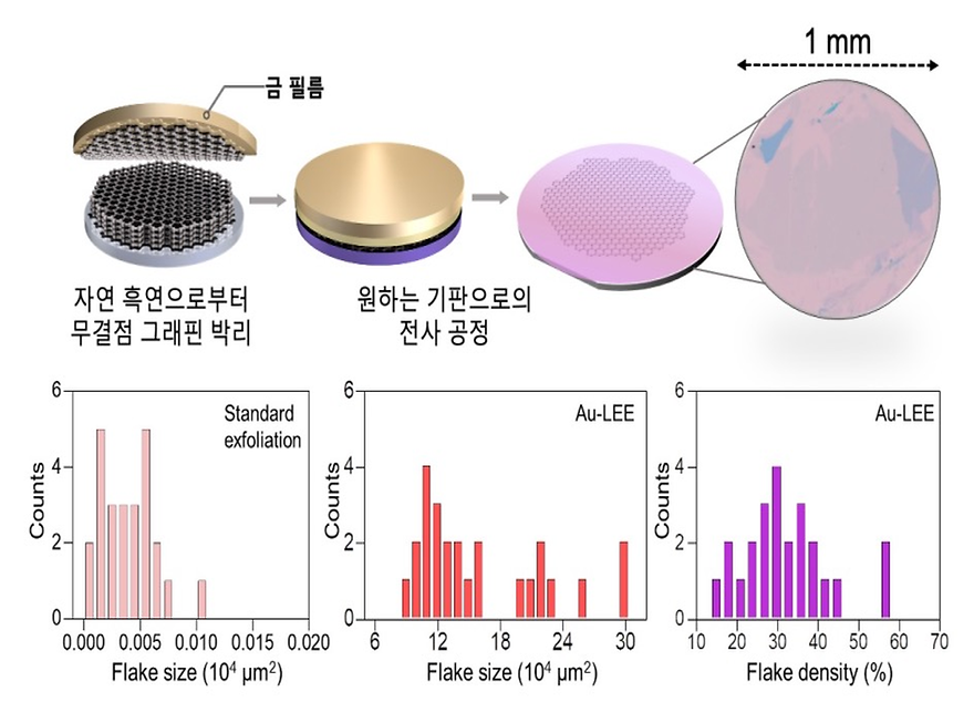
Professor Lee Jae-hyun of Ajou University has developed a new graphene exfoliation technique for graphite, a next-generation electron material.A joint research team involving professor Lee Jae-hyun (Department of Materials Science and Engineering, photo), Son Seok-kyun of Mokpo National University, and Cho Sung-ho, director of Samsung Display, announced that the team had developed a new technique of layer-engineered large-area exfoliation of graphene. The study was published in Science Advances on October 28th and titled, “Layer-engineered large-area exfoliation of graphene”. PhD student Moon ji-Yoon and Doctor Kim Min-soo from the University of Manchester participated as lead authors. Graphene, a transparent material with rubber-like flexibility, has received a lot of attention as a “dream material” for its outstanding electrical conductivity. These characteristics make graphene perfect for rollable TVs and smartphone screens. Graphene is a compound integration of carbon atoms that form a beehive shape. This monolayer material is so thin that 100,000 layers are equal to the diameter of a human hair.The conventional method of obtaining graphene sheets from graphite flakes required workers to repeatedly peel off layers of graphite crystals using cellophane tape. This was immensely dependent on worker skill and made it almost impossible to control monolayer graphene area, number of layers and yield.Professor Lee’s team succeeded in controlling, at the atom level, the crack propagation, especially size and direction, produced when peeling off layers using cellophane tape and obtaining the desired area and number of layers. According to Lee’s new method, a specific metal film is attached to graphite to selectively, rather than randomly, control the depth and direction of cracks. The research team’s finding enables production of layer-controlled graphene: from mm2-monolayer to double layer and up to 40 layers. The average area of monolayer graphene exfoliated using the new method is up to approximately 4200 times that of monolayer graphene exfoliated by the standard method. In addition, the density per unit area of monolayer graphene increased by a maximum of 6000 times, which enables higher yield. The recent study is expected to be an alternative method for preparing graphene, as obtaining fine quality exfoliated graphene is essential for commercialization. Research was sponsored by a grant from the Korean Ministry of Science and ICT and the National Research Foundation of Korea as part of their Basic Science and Engineering Lab Program and Beginning Researcher Program. 금필름Gold Film자연 흑연으로부터 무결점 그래핀 박리Exfoliation of top graphene from bulk crystal원하는 기판으로의 전사 공정Transfer to target substrate(Top) The exfoliation process of selective monolayer graphene from natural graphite flakes through attachment of gold film. (Bottom) Graphs comparing the size and density of monolayer graphene exfoliated using the conventional method and using the new method with gold film. The average area of monolayer graphene obtained using gold film is up to 4200 times the standard exfoliation method and up to 6000 times the density.
-
16
- 작성자OI***
- 작성일2020-12-18
- 7018
- 동영상동영상
-
A team led by Ajou University Professor Jeon Sang-min has found that a specific gene formerly considered helpful in prevention and treatment of cancer, in fact, stimulates its development and progression. Professor Jeon Sang-min (College of Pharmacy, photo) discovered that, contrary to traditional understanding, Nuclear factor E2-related factor 2 (NRF2) is a gene that stimulates cancer development and is also related to poor clinical outcomes, not at all a tumor suppressor gene. His study was published in Clinical Cancer Research on October 19th and entitled, “NRF2 activation promotes aggressive lung cancer and associates with poor clinical outcomes”. Professor Jeon Sang-min, PhD student Choi Eun-ji, US company Genentech, and a research team from Johns Hopkins Medical Institutions participated in the recent study, which was sponsored with a grant from the Korea National R&D Program for Cancer Control (Ministry of Health and Welfare) and the Basic Science Research Program (Individual Basic Science & Engineering Research Program) under the Ministry of Science, ICT and Future Planning.NRF2 has long been considered helpful in preventing and treating cancer as it was believed to reduce reactive oxygen species (ROS) once it is processed into a transcription factor that activates anti-oxidation pathways. However, several recent findings have suggested that NRF2 may actually contribute to tumor development, because in many cases of cancer, including cancer of the lung, NRF2 was activated.Another study also found that, in lung cancer cases, NRF2 activation occurred along with the mutation of STK11/LKB1, which are other tumor suppressor genes. Accordingly, the joint research team conducted experiments based on a genetically modified lung cancer mouse model (Kras/Keap1/Stk11-KO) and analyzed the results of the latest large-scale lung cancer clinical trials (OAK, IMpower131). The research team identified that, in the genetically modified mouse model, the activation of NRF2 stimulated lung cancer development and lowered survival rates. The team also found that the STK11 gene mutation increased ROS and stimulated the progression of lung cancer development. When STK11 mutation and NRF1 activation were both taking place, they suppressed ROS, further promoted lung cancer development and significantly lowered survival rates. The research team discovered that the reason NRF2 activation and STK11 mutation happen simultaneously in lung cancer cases is because NRF2 activation reduces oxidative stress incurred by STK11 mutation leading to cancer cell survival and growth. In conclusion, the study produced meaningful findings proving that NRF2 is a tumor oncogene, not a tumor suppressor gene. The team also analyzed recent clinical trials and found that lung cancer patients with active NRFs were highly likely to have poorer chemotherapy and immunotherapy outcomes than those who didn’t have active NRFs, and had significantly lower survival rates.Professor Jeon Sang-min stated “The study suggests a paradigm shift in the role of NRF2 in cancer. […] Many attempts have been made to develop an NRF2 stimulant for cancer prevention and treatment. However, our research has set the record straight and contributed to increasing interest on the development of an NRF2 inhibitor.”Professor Jeon’s research team is continuing efforts to be the first in developing such an NRF2 inhibitor drug. Professor Jeon participated in joint creation of SCL Therapeutics, a bio start-up, for clinical development of the self-discovered NRF2 inhibitor candidate. Currently, the lab is conducting pre-clinical trials.
-
14
- 작성자OI***
- 작성일2020-12-18
- 6107
- 동영상동영상
-
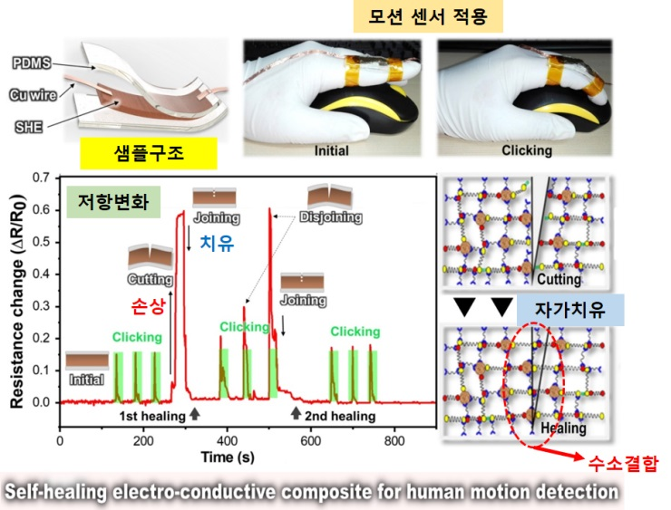
모션 센서 적용Motion detector applied샘플구조Sample structure저항변화Change in resistance치유Healing손상Damage자가치유Self-healing수소결합Hydrogen bondingA team of researchers led by Prof. Seo Hyung-tak (Departments of Materials Science and Engineering and Energy Systems Research) has successfully developed a new self-healing composite material and a sensor based on that material. Highly conductive and elastic, the new material is expected to have wide-ranging applications, including wearable electronics, soft robotics, and artificial skin.The composite invented by Prof. Seo’s team is made of a supramolecular polymer and copper microparticles, and the team developed an electronic wearable strain sensor capable of self-healing. The researchers’ work was published as the featured article in the September 7 online issue of Advanced Electronic Materials and entitled, “Intrinsically stretchable and self-healing electroconductive composite based on supramolecular organic polymer embedded with copper microparticles.” Rubaya Yeasmin, a doctoral candidate at Ajou, was listed as first author.The human skin is structured so that it detects damage quickly and activates self-restoring mechanisms to prevent the damage from worsening and facilitate healing. Inspired by this natural self-healing mechanism of organisms, researchers worldwide are searching for new materials capable of self-healing and restoration, and possessing electroconductivity and elasticity (stretchability). It takes significant skill and resources to develop new electronic materials capable of restoring themselves after damage without external intervention or processes. Once invented, such materials can exert far-reaching ripple effects on industry and society.In this project, the research team combined a supramolecular organic polymer and copper microparticles (1 μm = 1E-6m; for comparison, the average width of a hair strand is 100 μm). The resulting composite can be manufactured on a mass scale in aerosol and gel form. The copper concentration can also be adjusted to control electroconductivity of the final product. Supramolecular polymers support elastic and self-healing hydrogen bonding. The copper concentration can also be used to control the electric properties of semiconductors and conductors. The team has optimized the electrical properties of their composite so that it can continue to restore itself, notwithstanding multiple cuts. The most remarkable characteristic about the team’s product is its highly stretchable and self-healing structure, which renders it very similar to real skin. This material is resistant to tearing and can be stretched to 120 percent of its original length. Its electric and mechanical properties are also restored even after it has been cut. The team, in fact, demonstrated that the material recovered 90 percent of its mechanical properties and 100 percent of its electrical properties in just five minutes in the given environment.The team used the new material to develop a new wearable strain sensor capable of self-healing, whose workings it successfully demonstrated by attaching it to the fingers of human subjects. By deliberately cutting and damaging the sensor and gauging its reaction, the team also confirmed its ability to restore itself.Prof. Seo explained: “The self-healing material we’ve developed was made with affordable components and processes, without the need for great cost. A wide range of applications are possible beyond only wearable sensors, and include elastic IoT sensors, soft robotics, and industrial equipment.”The project was conducted in part thanks to the Research Support Program for New Researchers with Advanced Overseas Accomplishments, the Basic Research Support Program, and the BK21 Four Program from the Ministry of Science and ICT and the National Research Foundation of Korea.
-
12
- 작성자OI***
- 작성일2020-12-18
- 5143
- 동영상동영상

